- 您现在的位置:买卖IC网 > Sheet目录330 > IDT71V321L25TFI (IDT, Integrated Device Technology Inc)IC SRAM 16KBIT 25NS 64STQFP
IDT71V321/71V421S/L
High Speed 3.3V 2K x 8 Dual-Port Static RAM with Interrupts
Industrial and Commercial Temperature Ranges
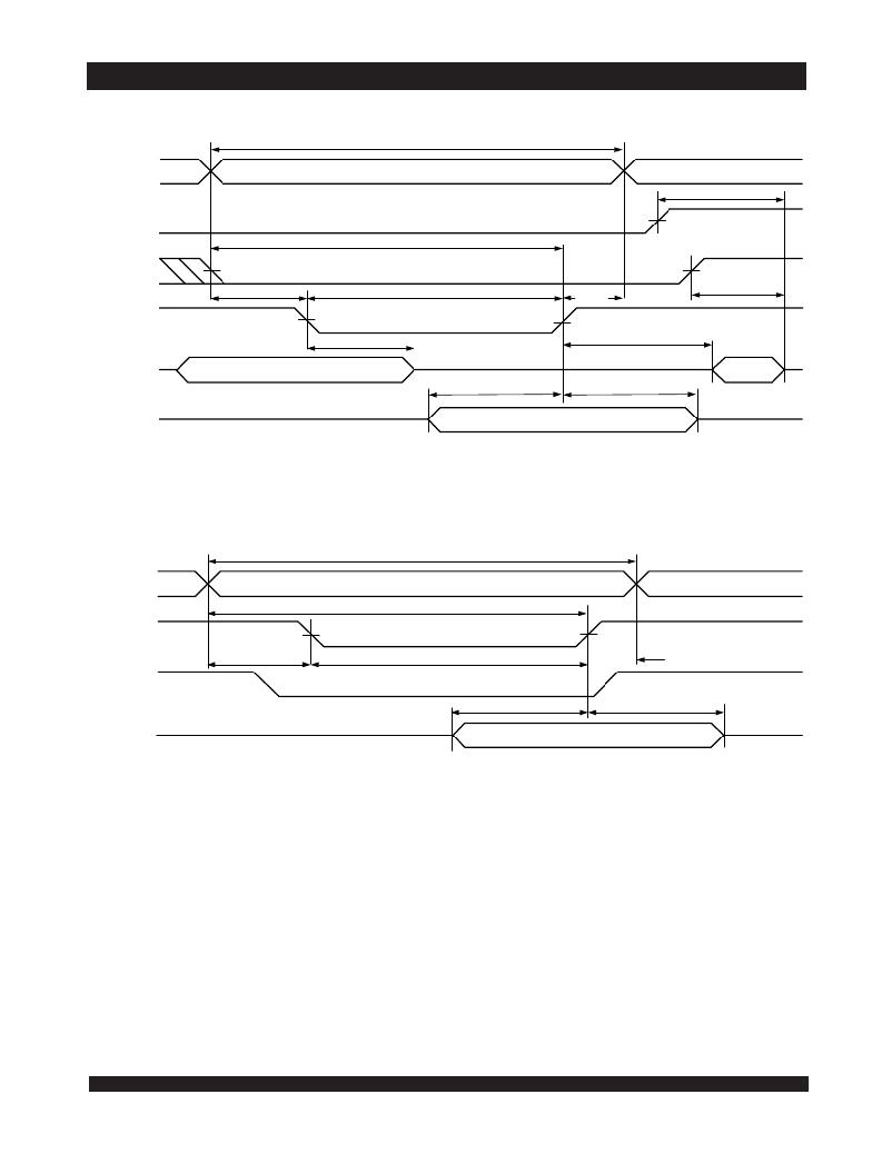
Timing Waveform of Write Cycle No. 1, (R/ W Controlled Timing) (1,5,8)
t WC
ADDRESS
t HZ (7)
OE
t AW
CE
t AS (6)
t WP (2)
t WR (3)
t HZ (7)
R/ W
t WZ (7)
t OW
DATA OUT
(4)
t DW
t DH
(4)
DATA IN
3026 drw 08
Timing Waveform of Write Cycle No. 2, ( CE Controlled Timing) (1,5)
t WC
ADDRESS
t AW
CE
t AS (6)
t EW (2)
t WR
(3)
R/ W
t DW
t DH
DATA IN
3026 drw 09
NOTES:
1. R/ W or CE must be HIGH during all address transitions.
2. A write occurs during the overlap (t EW or t WP ) of CE = V IL and R/W= V IL .
3. t WR is measured from the earlier of CE or R/ W going HIGH to the end of the write cycle.
4. During this period, the l/O pins are in the output state and input signals must not be applied.
5. If the CE LOW transition occurs simultaneously with or after the R/ W LOW transition, the outputs remain in the High-impedance state.
6. Timing depends on which enable signal ( CE or R/ W ) is asserted last.
7. This parameter is determined to be device characterization, but is not production tested. Transition is measured 0mV from steady state with the Output Test
Load (Figure 2).
8. If OE is LOW during a R/ W controlled write cycle, the write pulse width must be the larger of t WP or (t WZ + t DW ) to allow the I/O drivers to turn off data to be
placed on the bus for the required t DW . If OE is HIGH during a R/ W controlled write cycle, this requirement does not apply and the write pulse can be as short
as the specified t WP .
8
6.42
发布紧急采购,3分钟左右您将得到回复。
相关PDF资料
IDT71V3556SA166BGGI
IC SRAM 4MBIT 166MHZ 119BGA
IDT71V3559S85BQI
IC SRAM 4MBIT 85NS 165FBGA
IDT71V35761YSA200BGI
IC SRAM 4MBIT 200MHZ 119BGA
IDT71V3577S75BQG
IC SRAM 4MBIT 75NS 165FBGA
IDT71V3578S150PFGI
IC SRAM 4MBIT 150MHZ 100TQFP
IDT71V416L10PHGI
IC SRAM 4MBIT 10NS 44TSOP
IDT71V424S10YGI
IC SRAM 4MBIT 10NS 36SOJ
IDT71V432S5PFGI
IC SRAM 1MBIT 5NS 100TQFP
相关代理商/技术参数
IDT71V321L25TFI8
功能描述:IC SRAM 16KBIT 25NS 64STQFP RoHS:否 类别:集成电路 (IC) >> 存储器 系列:- 标准包装:72 系列:- 格式 - 存储器:RAM 存储器类型:SRAM - 同步 存储容量:9M(256K x 36) 速度:75ns 接口:并联 电源电压:3.135 V ~ 3.465 V 工作温度:-40°C ~ 85°C 封装/外壳:100-LQFP 供应商设备封装:100-TQFP(14x14) 包装:托盘 其它名称:71V67703S75PFGI
IDT71V321L35J
功能描述:IC SRAM 16KBIT 35NS 52PLCC RoHS:否 类别:集成电路 (IC) >> 存储器 系列:- 标准包装:72 系列:- 格式 - 存储器:RAM 存储器类型:SRAM - 同步 存储容量:9M(256K x 36) 速度:75ns 接口:并联 电源电压:3.135 V ~ 3.465 V 工作温度:-40°C ~ 85°C 封装/外壳:100-LQFP 供应商设备封装:100-TQFP(14x14) 包装:托盘 其它名称:71V67703S75PFGI
IDT71V321L35J8
功能描述:IC SRAM 16KBIT 35NS 52PLCC RoHS:否 类别:集成电路 (IC) >> 存储器 系列:- 标准包装:2,000 系列:MoBL® 格式 - 存储器:RAM 存储器类型:SRAM - 异步 存储容量:16M(2M x 8,1M x 16) 速度:45ns 接口:并联 电源电压:2.2 V ~ 3.6 V 工作温度:-40°C ~ 85°C 封装/外壳:48-VFBGA 供应商设备封装:48-VFBGA(6x8) 包装:带卷 (TR)
IDT71V321L35JG
功能描述:IC SRAM 16KBIT 35NS 52PLCC RoHS:是 类别:集成电路 (IC) >> 存储器 系列:- 标准包装:72 系列:- 格式 - 存储器:RAM 存储器类型:SRAM - 同步 存储容量:9M(256K x 36) 速度:75ns 接口:并联 电源电压:3.135 V ~ 3.465 V 工作温度:-40°C ~ 85°C 封装/外壳:100-LQFP 供应商设备封装:100-TQFP(14x14) 包装:托盘 其它名称:71V67703S75PFGI
IDT71V321L35JG8
制造商:Integrated Device Technology Inc 功能描述:IC SRAM 16KBIT 35NS 52PLCC
IDT71V321L35PF
功能描述:IC SRAM 16KBIT 35NS 64TQFP RoHS:否 类别:集成电路 (IC) >> 存储器 系列:- 标准包装:72 系列:- 格式 - 存储器:RAM 存储器类型:SRAM - 同步 存储容量:9M(256K x 36) 速度:75ns 接口:并联 电源电压:3.135 V ~ 3.465 V 工作温度:-40°C ~ 85°C 封装/外壳:100-LQFP 供应商设备封装:100-TQFP(14x14) 包装:托盘 其它名称:71V67703S75PFGI
IDT71V321L35PF8
功能描述:IC SRAM 16KBIT 35NS 64TQFP RoHS:否 类别:集成电路 (IC) >> 存储器 系列:- 标准包装:72 系列:- 格式 - 存储器:RAM 存储器类型:SRAM - 同步 存储容量:9M(256K x 36) 速度:75ns 接口:并联 电源电压:3.135 V ~ 3.465 V 工作温度:-40°C ~ 85°C 封装/外壳:100-LQFP 供应商设备封装:100-TQFP(14x14) 包装:托盘 其它名称:71V67703S75PFGI
IDT71V321L35PFGI
制造商:Integrated Device Technology Inc 功能描述:IC SRAM 16KBIT 35NS 64TQFP
